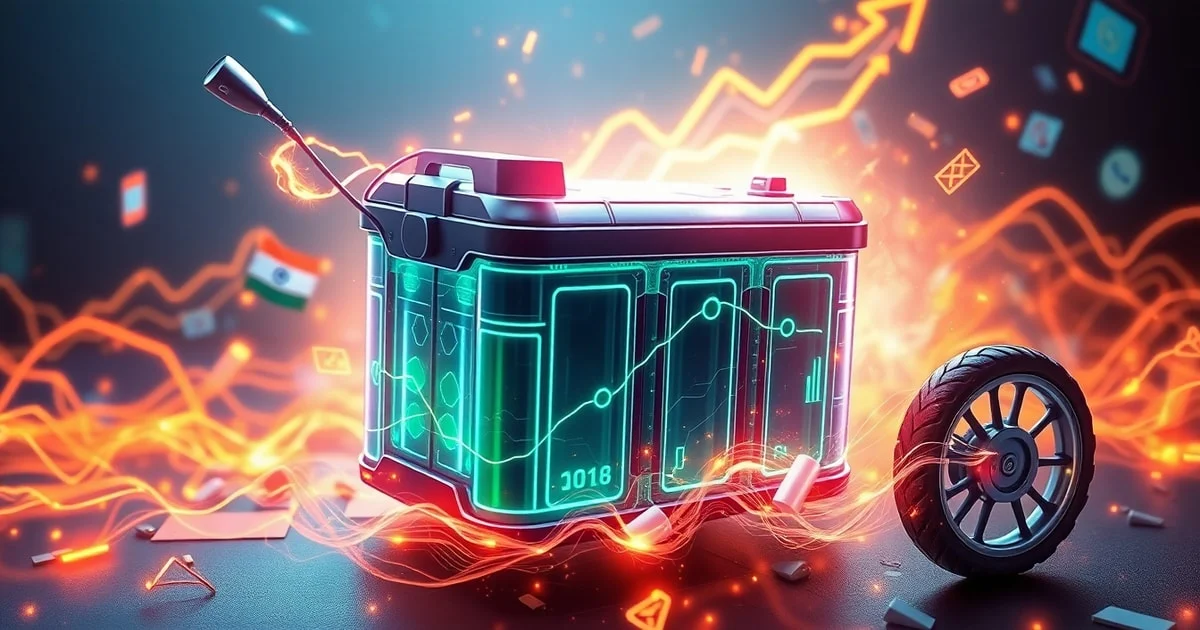
India Breaks Ground on 3D Glass Chip Manufacturing, Boosts Tech

In a landmark moment for its burgeoning technology sector, India Breaks Ground on 3D Glass Chip Manufacturing, marking a crucial step towards self-reliance and global leadership in advanced semiconductor technology. This significant development, centered around the establishment of the nation's first advanced 3D chip packaging facility, is poised to profoundly impact India's digital economy and strategic capabilities. The project signals a deeper shift in the global semiconductor supply chain, as India diversifies its manufacturing base and targets higher-value segments of the ecosystem. This groundbreaking initiative in Odisha represents a major leap, boosting India's indigenous capabilities in chip production.
- Background and Significance of 3D Glass Chip Manufacturing
- Key Details of India's Groundbreaking Initiative
- Expert Perspectives on India's Semiconductor Ambitions
- Broader Impact and Future Outlook
- Conclusion: India Breaks Ground on 3D Glass Chip Manufacturing, Paving the Way Forward
- Frequently Asked Questions
- Further Reading & Resources
Background and Significance of 3D Glass Chip Manufacturing
India's recent groundbreaking on its first advanced 3D chip packaging facility in Odisha underscores a strategic pivot in its quest for semiconductor independence and technological prowess. For years, India has been a significant player in chip design, but manufacturing capabilities have lagged behind. This new initiative, therefore, represents a crucial step in building a comprehensive domestic semiconductor ecosystem. The move is a direct response to global supply chain vulnerabilities highlighted in recent years and aligns with the nation's ambitious Atmanirbhar Bharat (Self-Reliant India) vision.
What are 3D Glass Chips?
Traditional semiconductor manufacturing primarily relies on silicon wafers and planar (2D) packaging, where components are laid out side-by-side. In contrast, 3D glass chip technology utilizes glass substrates and advanced 3D heterogeneous integration (3DHI) packaging. This cutting-edge approach allows for multiple chip components to be vertically integrated or stacked, dramatically increasing computing power within the same physical footprint. Glass substrates offer several key advantages over conventional materials, including better thermal management, higher interconnect density, improved reliability, enhanced thermal stability, lower signal loss, and greater precision for advanced nodes. This technology is particularly vital for next-generation applications demanding high performance and energy efficiency.
Why India is Investing in Semiconductor Manufacturing
India's push into semiconductor manufacturing is driven by a confluence of economic, strategic, and technological imperatives. Economically, the global semiconductor market is projected to reach substantial figures, with India's market alone expected to hit $103 billion by 2030. Building domestic manufacturing capabilities reduces reliance on imports, saves foreign exchange, and creates a significant number of high-skilled jobs. Strategically, semiconductors are critical components in almost every modern electronic device, from consumer gadgets to defense systems. Developing an indigenous supply chain enhances national security and reduces geopolitical vulnerabilities associated with relying on external sources. Technologically, investing in advanced packaging like 3D glass chips positions India at the forefront of innovation, allowing it to capture higher value in the global semiconductor value chain, moving beyond mere assembly and testing.
Key Details of India's Groundbreaking Initiative
The recently initiated project is more than just a manufacturing unit; it is a strategic investment in a high-tech future. The facility represents a crucial component of India's broader semiconductor mission, which aims to establish a comprehensive ecosystem from design to fabrication and packaging.
Strategic Location and Investment
The advanced 3D chip packaging facility is being established by Heterogeneous Integration Packaging Solutions, an Indian subsidiary of the US-based 3D Glass Solutions Inc. (3DGS). This significant project is located at Info Valley in Bhubaneswar, Odisha. The total investment for this state-of-the-art unit is approximately ₹1,943 crore, equivalent to about US$209 million. This substantial investment underscores the commitment from both the private sector and government to propel India's semiconductor ambitions forward. The Odisha Chief Minister Mohan Majhi and Union Electronics and IT Minister Ashwini Vaishnaw were present at the groundbreaking ceremony, highlighting the project's national importance.
Technological Advancements and Partnerships
The Odisha plant will specialize in advanced 3D heterogeneous integration (3DHI) using glass substrates, a technology where India has previously relied heavily on imports. The core of the project leverages 3DGS's APEX glass-ceramic packaging platform, which is backed by over 100 patents across 31 active patent families globally. These patents encompass materials engineering, manufacturing processes, device architectures, and system-level integration, ensuring a robust technological foundation. This advanced packaging technology is critical for next-generation applications demanding high performance and energy efficiency. This initiative is supported by significant global investors, including Intel Capital, Lockheed Martin Ventures, Applied Ventures, and Walden Catalyst Ventures, reflecting the strategic importance and potential of the underlying technology. The facility aims to support critical high-performance applications.
Anticipated Production Capacity and Timelines
Once fully operational, the facility is designed for a substantial annual production capacity. It is projected to produce 69,600 glass panel substrates, 50 million assembled units, and 13,200 3DHI modules each year. The company has set ambitious targets, with commercial production expected to commence by August 2028, and full-scale output anticipated by August 2030. This aggressive timeline demonstrates the urgency and commitment behind establishing India as a serious player in the advanced semiconductor packaging sector. The IT minister, Ashwini Vaishnaw, has also indicated plans to double the capacity of the plant after the completion of its first phase, signifying strong growth projections and confidence in the project's success.
Expert Perspectives on India's Semiconductor Ambitions
The establishment of this advanced 3D glass chip packaging facility has garnered significant attention from industry experts and policymakers alike. It is viewed not merely as an industrial project but as a foundational step for India's future technological landscape.
Economic Impact and Job Creation
The economic ramifications of this venture are expected to be substantial. Beyond boosting India's domestic technological capabilities, the facility is projected to create over 2,500 direct and indirect employment opportunities. This influx of jobs will stimulate local economies, particularly in Odisha, which is diversifying its industrial base. Union Electronics and IT Minister Ashwini Vaishnaw hailed the groundbreaking as a "historical day" for Odisha, emphasizing its emergence as both an IT hub and an electronics manufacturing destination. The India Electronics and Semiconductor Association (IESA) has welcomed the inauguration, calling it a clear sign of India's shift from policy intent to concrete execution in semiconductors. Such developments are critical as India aims to become a 103 billion semiconductor market by 2030.
Geopolitical Implications and Supply Chain Resilience
From a geopolitical standpoint, the facility plays a crucial role in enhancing global semiconductor supply chain resilience. The COVID-19 pandemic and subsequent geopolitical tensions highlighted the fragility of highly concentrated supply chains. By developing domestic capabilities in advanced packaging, India aims to reduce its reliance on imports and secure critical components for strategic sectors such as artificial intelligence, 5G networks, defense systems, data centers, and high-performance computing. This strategic move positions India as a more dependable and diversified source for semiconductor technologies, a factor that holds increasing importance in the current global climate. IT Secretary S Krishnan underscored the significance, stating that this project can truly put India "on the map" in terms of advanced chip packaging, representing truly advanced and novel technology.
Broader Impact and Future Outlook
The groundbreaking for India's 3D glass chip manufacturing unit is not an isolated event but a part of a larger, coordinated national effort under the India Semiconductor Mission (ISM). This mission, launched in 2021 with an outlay of ₹76,000 crore, aims to build a full-stack chip ecosystem in the country.
Fostering an Indigenous Semiconductor Ecosystem
The Odisha facility is one of ten semiconductor projects approved under the ISM across six states, with cumulative investments exceeding ₹1.6 lakh crore (approximately $18.25 billion). These projects include not only fabrication plants (like the one being built by the Tata Group in Dholera, Gujarat) but also assembly, testing, marking, and packaging (ATMP/OSAT) units, and design-linked incentives. The emphasis on advanced packaging, particularly heterogeneous integration using glass substrates, signifies India's ambition to move beyond conventional assembly processes and target more IP-intensive segments of semiconductor manufacturing. This will help foster an indigenous ecosystem, encouraging local talent, research, and development in cutting-edge semiconductor technologies. Furthermore, Odisha now holds the unique distinction of being the first Indian state to host both a compound semiconductor fabrication unit (SiCSem) and an advanced 3D chip packaging facility based on glass substrates. This regional specialization highlights a focused approach to developing key areas of the semiconductor value chain.
Global Competition and Collaboration
While India is making significant strides, the global semiconductor landscape remains highly competitive. The country's strategy involves both fostering domestic capabilities and engaging in strategic collaborations. The partnership with US-based 3D Glass Solutions Inc. (3DGS) exemplifies this approach, bringing world-class technology and intellectual property to India. This blend of global expertise with Indian execution capability and public sector support suggests a maturing semiconductor strategy, aiming for higher-value segments rather than just low-cost manufacturing. India's proactive policies, including revised Special Economic Zone (SEZ) rules to ease the establishment of semiconductor manufacturing units, are designed to attract further international investment and partnerships. The Delhi government is also drafting a semiconductor policy to establish the capital as a hub for chip design and research, further diversifying India's contributions to the global semiconductor industry.
Conclusion: India Breaks Ground on 3D Glass Chip Manufacturing, Paving the Way Forward
The groundbreaking of India's first advanced 3D chip packaging facility in Odisha marks a pivotal moment in the nation's technological journey. By strategically investing in cutting-edge technologies like 3D glass chip manufacturing and fostering robust domestic and international partnerships, India is not only enhancing its self-reliance but also positioning itself as a critical player in the global semiconductor ecosystem. This initiative, backed by the India Semiconductor Mission, promises to unlock significant economic opportunities, create high-skilled jobs, and bolster India's strategic capabilities in an increasingly digital world. This is a clear demonstration of India's commitment to moving from policy formulation to tangible execution in the high-stakes semiconductor sector, with long-term implications for innovation and economic growth.
Frequently Asked Questions
Q: What are 3D glass chips and their advantages?
A: 3D glass chips utilize a cutting-edge approach that allows for multiple chip components to be vertically integrated or stacked on glass substrates. This technology offers significant advantages over traditional 2D silicon, including better thermal management, higher interconnect density, improved reliability, and lower signal loss, making them ideal for high-performance computing and AI applications.
Q: Where is India's new 3D glass chip manufacturing facility located?
A: India's first advanced 3D chip packaging facility is being established by Heterogeneous Integration Packaging Solutions, an Indian subsidiary of US-based 3D Glass Solutions Inc. (3DGS), in Info Valley, Bhubaneswar, Odisha. This strategic location aims to bolster the region's technological and industrial base.
Q: What is the significance of this project for India?
A: This groundbreaking project is a crucial step towards India's self-reliance in the semiconductor sector, reducing dependence on imports and enhancing national security. It is expected to create over 2,500 direct and indirect jobs, stimulate economic growth, and position India as a key player in advanced semiconductor technology on the global stage.