Huawei Unveils Revolutionary Semiconductor Tech to Bypass Sanctions
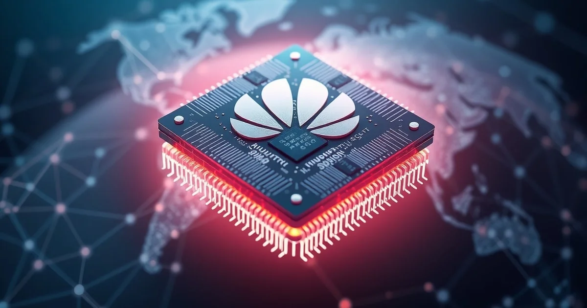
In a move set to redefine the global semiconductor landscape, Chinese telecommunications giant Huawei has officially announced a groundbreaking innovation designed to circumvent existing international trade restrictions. At the prestigious 2026 IEEE International Symposium on Circuits and Systems (ISCAS) held in Shanghai on May 25, 2026, Huawei unveiled its "Tau (τ) Scaling Law" and a revolutionary chip architecture dubbed "LogicFolding." This announcement marks a pivotal moment, as Huawei Unveils Revolutionary Semiconductor Tech with the ambitious goal of achieving 1.4-nanometer equivalent transistor density by 2031, despite facing significant limitations on access to advanced Extreme Ultraviolet (EUV) lithography equipment. This strategic pivot highlights the company's determination to forge an independent path in high-performance computing, fostering technological sovereignty in an increasingly complex geopolitical environment.
Background on Semiconductor Challenges
The global semiconductor industry has been navigating a turbulent period marked by unprecedented challenges. From persistent supply chain disruptions to intensified geopolitical rivalries, the landscape for chip manufacturing is in constant flux. These external pressures have pushed nations and corporations alike to re-evaluate their long-term strategies, emphasizing resilience and domestic production capabilities. The pursuit of advanced chip technology has become a central arena for economic and national security competition. For more insights into these dynamics, read our analysis on Geopolitics and Semiconductor Supply Chains.
The Global Chip Shortage
For several years, the world has grappled with a severe chip shortage, impacting industries from automotive to consumer electronics. This scarcity was exacerbated by a confluence of factors, including surging demand for digital technologies during the pandemic, unexpected factory shutdowns, and logistical bottlenecks. Even in 2025, the semiconductor industry, while poised for significant growth, continues to grapple with the need for expanded manufacturing capacity and improved supply chain robustness. The industry is projected to reach approximately $697 billion in 2025, with an 11% year-over-year increase driven by strong demand in data centers and AI technologies. However, maintaining this growth requires overcoming persistent headwinds, including challenges in talent acquisition and geopolitical stability.
Geopolitical Landscape and Tech Sovereignty
The U.S.-China semiconductor rivalry has escalated significantly in recent years, reaching unprecedented levels by 2025. This rivalry has fundamentally restructured global supply chains, with the U.S. imposing tariffs and export controls on advanced semiconductor technology and China retaliating with rare earth export controls. The restrictions aim to limit China's access to cutting-edge AI computing power, which Washington views as having national security implications. In response, Chinese companies, including Huawei, have intensified their investments in domestic chip production and alternative technological infrastructures. This ongoing "chip war" underscores the critical importance of technological sovereignty, with nations striving to reduce reliance on foreign suppliers for essential components.
Huawei Unveils Revolutionary Semiconductor Tech: The Details
Huawei's recent announcement at the 2026 IEEE International Symposium on Circuits and Systems (ISCAS) has sent ripples throughout the technology world, signaling a bold new direction for semiconductor development. The company introduced a novel framework that seeks to move beyond traditional limitations imposed by physical scaling, offering a potential pathway to high-performance chips without direct access to the most advanced lithography equipment. This strategy is a direct response to the export controls that have impacted Huawei since 2019, demonstrating an innovative approach to overcoming technological barriers.
Breakthrough Innovations and Key Features
Central to Huawei's new semiconductor strategy are two interconnected concepts: the Tau (τ) Scaling Law and the LogicFolding architecture.
The Tau (τ) Scaling Law: proposes a fundamental shift in how the semiconductor industry guides its future development. Instead of strictly adhering to Moore's Law, which focuses on the geometric scaling and physical shrinking of transistors, the Tau Scaling Law emphasizes time (τ) scaling. This principle guides the evolution of semiconductors and electronic systems by continuously compressing signal propagation delay and steadily improving transistor density through architectural optimizations.
Complementing this new law is Huawei's innovative LogicFolding architecture: This proprietary chip design moves beyond the conventional two-dimensional layout of circuits. Instead, LogicFolding involves vertically stacking and reorganizing logic circuits into multiple layers. By "folding" circuits onto themselves, Huawei aims to shorten internal signal paths significantly. This reduction in the physical distance between logic gates directly addresses latency and power inefficiencies inherent in complex, flat silicon layouts. Huawei claims this approach can deliver a remarkable 55% increase in transistor density and a 41% boost in power efficiency on the exact same manufacturing node, without needing to decrease transistor size.
How Huawei Achieved This
Huawei's journey to this breakthrough has been a clandestine effort spanning over six years, during which the company secretly designed and produced 381 chips based on their new blueprint, validating the engineering principles. The core of their achievement lies in architectural innovation rather than relying solely on extreme ultraviolet (EUV) lithography systems, which are currently restricted to Huawei due to sanctions. By focusing on optimizing the overall chip efficiency through signal delay reductions, architectural redesigns, and system-level performance improvements, Huawei is attempting to squeeze significantly more performance and density from existing manufacturing capabilities.
The concept of stacking chips is not entirely new; industry leaders like TSMC already employ advanced packaging technologies. However, Huawei is proposing a more aggressive and fundamental redesign of the chip architecture itself with LogicFolding. This involves utilizing advanced packaging techniques like 2.5D and 3D-IC to combine multiple semiconductor chips into a single, more capable, and power-efficient electronics package. To understand the broader impact of such innovations, explore our deep dive into The Rise of Advanced Packaging in Semiconductor Design. This strategic reorientation allows Huawei to enhance performance by improving how data moves across the chip, rather than solely depending on the physical shrinking of transistors, a path increasingly constrained by the laws of physics and costly EUV technology.
Potential Impact on the Global Tech Industry
Huawei's bold declaration has ignited discussions about its potential ramifications across the global technology sector. The company's innovative approach could reshape competitive dynamics, influence national security considerations, and potentially alter the trajectory of future semiconductor development. This development is particularly significant given the ongoing efforts by various nations to bolster their domestic semiconductor capabilities and reduce supply chain vulnerabilities.
Competition and Market Dynamics
If Huawei's LogicFolding architecture and Tau Scaling Law prove successful and scalable, they could dramatically impact the competitive landscape. Currently, companies like TSMC and Samsung are at the forefront of traditional geometric scaling, with TSMC aiming for 1.4nm mass production by 2028. Huawei’s projected 1.4nm-equivalent density by 2031, while still lagging TSMC by a few years in pure node size, represents a substantial narrowing of the technological gap that currently exists due to sanctions. This could allow Huawei to compete more effectively in high-end markets, particularly for smartphones and AI accelerators.
The commercial debut of LogicFolding in the upcoming Kirin smartphone chips for the Mate 90 series later in 2026, followed by its integration into Ascend AI processors and AI data centers by 2030, indicates Huawei's intent to rapidly deploy this technology across its product portfolio. This could intensify competition in the AI chip market, where Nvidia currently holds a dominant position but faces challenges with H200 shipments due to regulatory limbo. For further details on the evolving landscape of computing, check out our article on AI Chips and the Future of Data Centers. Huawei's push could also spur other Chinese firms to accelerate their own technological development, fostered by a renewed sense of confidence in domestic innovation.
Implications for National Security and Supply Chains
The geopolitical implications of Huawei's semiconductor breakthrough are profound. For Beijing, this achievement represents a major symbolic and practical victory in its quest for technological self-sufficiency and reduced dependence on foreign technology. By developing a viable alternative path to advanced chip performance, Huawei could mitigate the impact of US sanctions, which were designed to restrict China's access to strategic technologies.
This development further fragments the global semiconductor supply chain, pushing countries toward "friend-shoring" strategies where companies establish manufacturing in geopolitically aligned nations. The ongoing US-China tech war has already led to a bifurcated market, and Huawei's innovation could accelerate this trend, leading to distinct technological ecosystems. While it could enhance China's national security by securing its domestic chip supply, it also raises questions about global interoperability and collaboration in future technology development.
Future of Semiconductor Development
Huawei's Tau Scaling Law and LogicFolding architecture challenge the long-held paradigm of Moore's Law. For decades, the industry has relied on shrinking transistor sizes to improve performance. However, as chips approach the physical limits of miniaturization, and as EUV lithography becomes prohibitively expensive and politically restricted for some, alternative approaches are becoming increasingly critical.
Huawei's focus on architectural optimization, signal delay reduction, and vertical stacking represents a significant departure, suggesting that future advancements may come more from innovative design and packaging than from pure lithographic scaling. This could inspire other industry players to explore similar unconventional pathways, fostering a new era of diverse innovation in semiconductor research and development. The industry's pivot towards advanced packaging technologies, already a significant trend, is likely to accelerate further as companies seek to deliver more capability in smaller, more power-efficient configurations.
Expert Analysis and Industry Reactions
The announcement from Huawei has been met with a mix of excitement and cautious skepticism across the global semiconductor industry. Experts are dissecting the technical claims and assessing the practical viability of Huawei's proposed solutions, weighing their potential against the entrenched dominance of traditional fabrication methods. The implications for intellectual property, market adoption, and long-term economic impact are central to ongoing debates.
What Analysts Are Saying
Industry analysts recognize the strategic importance of Huawei's announcement, especially in the context of geopolitical pressures. Some view LogicFolding and the Tau Scaling Law as a revolutionary attempt to move beyond Moore's Law, representing a genuine leap forward for China's semiconductor capabilities. The ability to achieve 1.4nm-equivalent transistor density through architectural redesign, rather than solely through advanced lithography, is seen as a clever workaround to sanctions.
Others, however, approach the claims with more caution. They point out that while the concept of stacking technologies isn't new, Huawei's aggressive redesign of the chip architecture itself faces significant engineering challenges. These include manufacturing complexity, effective heat dissipation in multi-layered structures, and ensuring efficient power delivery. There is also the question of whether this technology can be deployed economically and at scale to truly challenge market leaders like TSMC, which is already working on true 1.4nm chips. The term "1.4 nanometer equivalent" itself has drawn scrutiny, with some noting that modern node names are often more about branding than precise physical measurements.
Challenges and Skepticism
Despite the audacious claims, Huawei still faces considerable hurdles. The company has not yet publicly revealed every technical detail of its LogicFolding architecture, leading to some uncertainty about its full capabilities and limitations. While the initial commercial deployment in Kirin chips is expected soon, scaling this technology to high-volume production for diverse applications, especially for advanced AI processors and data centers, will be a monumental task. The semiconductor fabrication process is incredibly complex, requiring highly specialized plants and taking many weeks, even for established methods.
Furthermore, the industry is already investing heavily in advanced packaging and next-generation lithography. For example, NVIDIA and TSMC are collaborating to integrate AI into fabs to advance semiconductor design and manufacturing, using GPU-accelerated computational lithography and vision AI for defect inspection. This indicates that while Huawei explores alternative paths, competitors are simultaneously pushing the boundaries of traditional methods and leveraging AI to optimize production. The long-term economic viability and mass production capacity of Huawei's new approach will be critical factors in determining its ultimate success and broader impact on the global market.
Conclusion
Huawei's unveiling of its Tau Scaling Law and LogicFolding architecture represents a significant and potentially transformative moment in the global semiconductor industry. By proposing a paradigm shift from traditional geometric scaling to an emphasis on architectural innovation and vertical integration, Huawei is directly addressing the formidable challenges posed by international sanctions and the physical limits of Moore's Law. This bold strategy underscores the company's commitment to achieving technological self-sufficiency and securing a competitive edge in advanced chip development. While the road ahead is undoubtedly complex, marked by engineering hurdles and the need for scalable, cost-effective production, this announcement firmly places Huawei Unveils Revolutionary Semiconductor Tech at the forefront of the ongoing debate about the future of high-performance computing. Its success could not only redefine Huawei's position but also inspire a new wave of innovation across the entire semiconductor ecosystem, fostering diverse pathways to next-generation chip performance.
Frequently Asked Questions
Q: What is Huawei's "LogicFolding" architecture?
A: LogicFolding is a proprietary chip design that vertically stacks and reorganizes logic circuits into multiple layers. This "folding" shortens internal signal paths, aiming for significant increases in transistor density and power efficiency on existing manufacturing nodes without shrinking transistor size.
Q: How does the "Tau Scaling Law" differ from Moore's Law?
A: Moore's Law focuses on geometric scaling and physically shrinking transistors. The Tau Scaling Law, however, emphasizes time (τ) scaling, guiding semiconductor evolution by continuously compressing signal propagation delay and improving transistor density through architectural and system-level optimizations.
Q: Will Huawei's new technology help it bypass US sanctions?
A: Huawei intends for LogicFolding and Tau Scaling Law to circumvent US sanctions by achieving advanced performance through architectural innovation rather than reliance on restricted EUV lithography. This strategy aims to foster technological independence for high-performance computing.